Dicing
Entrust the professionals at TAMA Electronics with your glass, quartz, or ceramic cutting. We will propose the optimal machining method depending on your requirements - whether using dicing tape or wax.
What is Dicing?
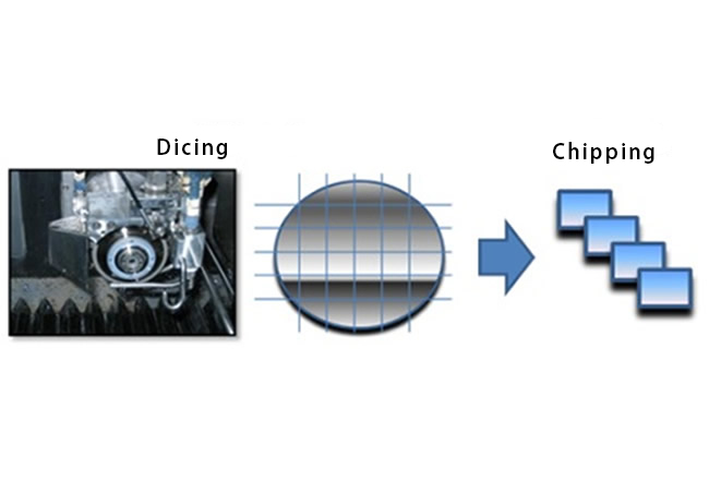
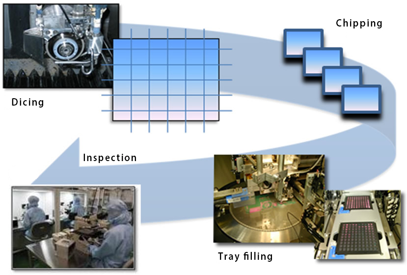
A diamond blade is used to cut the substrate into cubes. Our equipment is capable of machining semiconductor wafers, optical glass parts, and substrates made of various materials including ceramic into sizes as small as 0.5 mm.
We set our conditions to match those of your product specifications. Dicing tape offers cost advantages. On the other hand, wax and other materials are effective when precise external dimensional accuracy is required or when dicing substrates with different shapes.
Dicing
The professionals at TAMA Electronics are truly experts when it comes to dicing materials - thanks to our many years of experience in dicing semiconductor silicon substrates.
List of materials we handle
| Thickness | Min | Max |
|---|---|---|
| Glass | 0.5mm~ | ~5.0mm |
| Ceramic | 1.0mm~ | ~2.0mm |
| Silicon substrates | 0.2mm~ | ~1.0mm |
| Silicon and mold (laminate material) | 1.0mm~ | ~2.0mm |
| SiC (silicon carbide) | 1.0mm~ | ~2.0mm |
Glass dicing
We are here to meet your needs when it comes to dicing and grooving IR/UV cut filters and other optical glass substrates or quartz substrates - from trial products to small lots and mass production.
Ceramic dicing
We are capable of dicing materials such as alumina and other fine ceramics. We also have experience of dicing ceramic-made laminate package substrates. We are committed to meeting your needs when it comes to dicing and grooving alumina substrates - from trial products to small lots and mass production. We also have recent experience in dicing SiC (silicon carbide) substrates.
Thick/different material laminate wafer dicing
We use high output spindle slicers and dedicated thick object dicers for substrates with a thickness from 3 to 5 mm.
Crystal dicing
TAMA Electronics' unique technology allows us to cut KBr and other deliquescent crystal - without altering its properties. We can also apply moisture prevention coating to machined chips to prevent deliquescence. (* Some technologies currently under development.)
Dicing Process
Dicing example 1
Dicing example 2
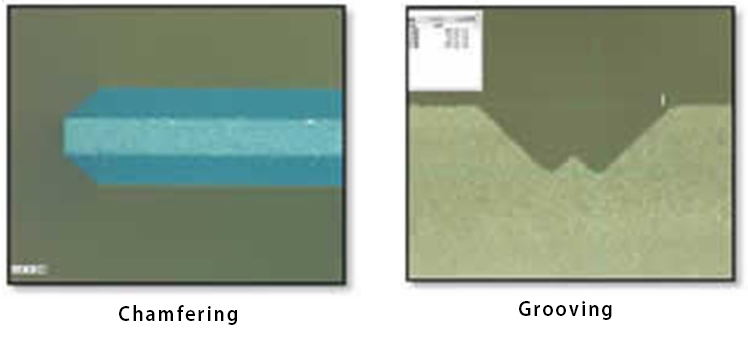
Our equipment is capable of chamfering, V-grooving, and other forms of special machining - and we can even provide quartz dicing of substrates up to 5.0 mm thick.
SiC Dicing
We have a long track record of dicing SiC (silicon carbide) wafers.
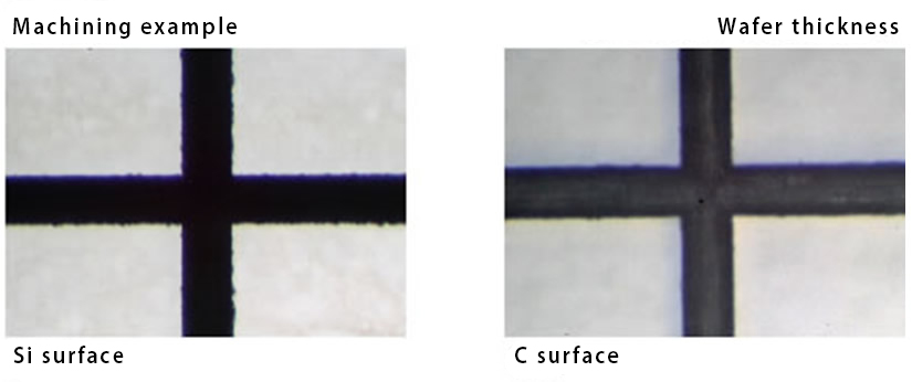
Machining quality
Chipping: < 20 µm (Si surface, C surface)
Machinable size
Wafer size: 2 to 6 inch
Wafer thickness: Up to 2.0 mm
Machining chip size: From 1.0 mm
Machining environment
Cleanroom: Design value of class 10,000 (actual value < 1,000)
Cutting fluid: Pure water with a specific resistance of 18 MΩ managed and used reduced to 0.7 MΩ with a CO2 bubbler
* We perform test machining. Please feel free to contact us.
Our Ceramic Dicing (Cutting) Technology
Slicing
At TAMA Electronics, we apply the dicing technology we have developed over many years toward cutting glass, ceramic, and other thick products.
Using slicers and dicers optimal for machining thick substrates allows us to machine substrates up to 24 mm thick.
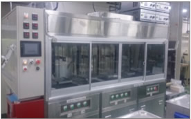
We can also cut using wax to further improve machining precision. After cutting we subject substrates to a thorough ultrasonic cleaning to eliminate any remaining wax or other substances. This delivers quality you can trust.
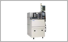
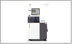
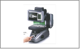
| Supported workpiece size | Square workpieces | Up to 90 mm across (up to 200 mm across with modified stage) |
|---|---|---|
| Round workpieces | Up to 4 inch (up to 8 inch with modified stage) | |
| Maximum cutting thickness | Up to 24 mm (including base substrate) | |
We offer integrated services for ceramics and other materials that cover everything from slicing to grinding and dicing.
| Supported workpiece thickness | Up to 100 mm * Please contact us for other thicknesses |
|---|
